Pcb Panel Design Tool

Top Five Circuit Board Design Apps Pcb Design
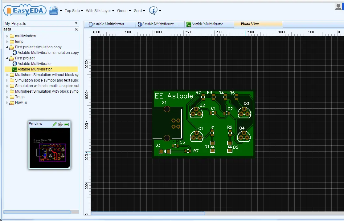
Build Pcb Online Using Web Based Eda Tools
Top Best Pcb Layout And Design Software For Macintosh

Pcb Design Procedures Pcb Design Schematic Design Tool Design
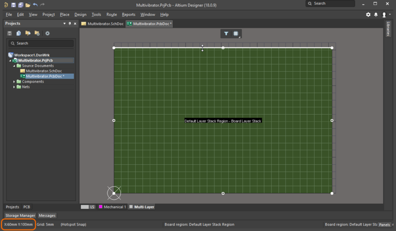
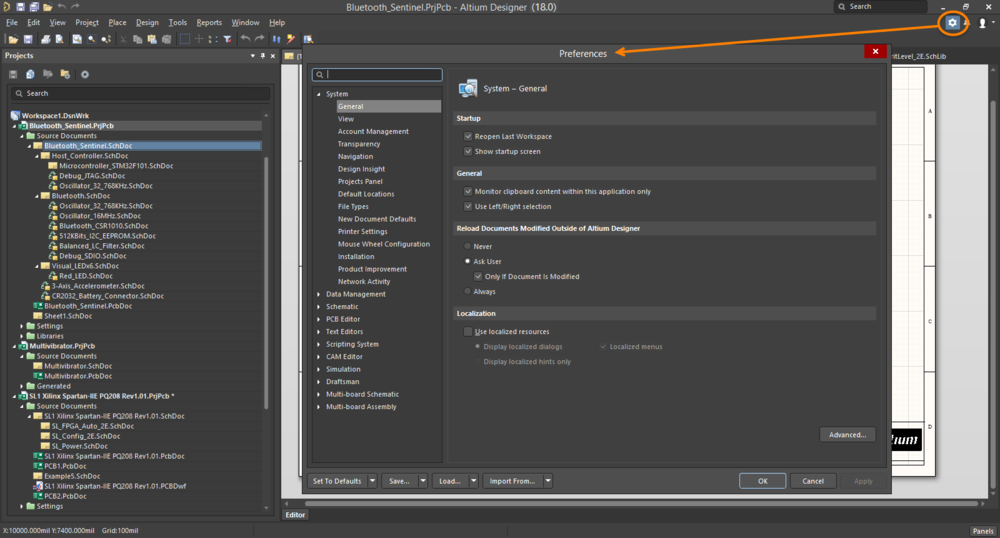
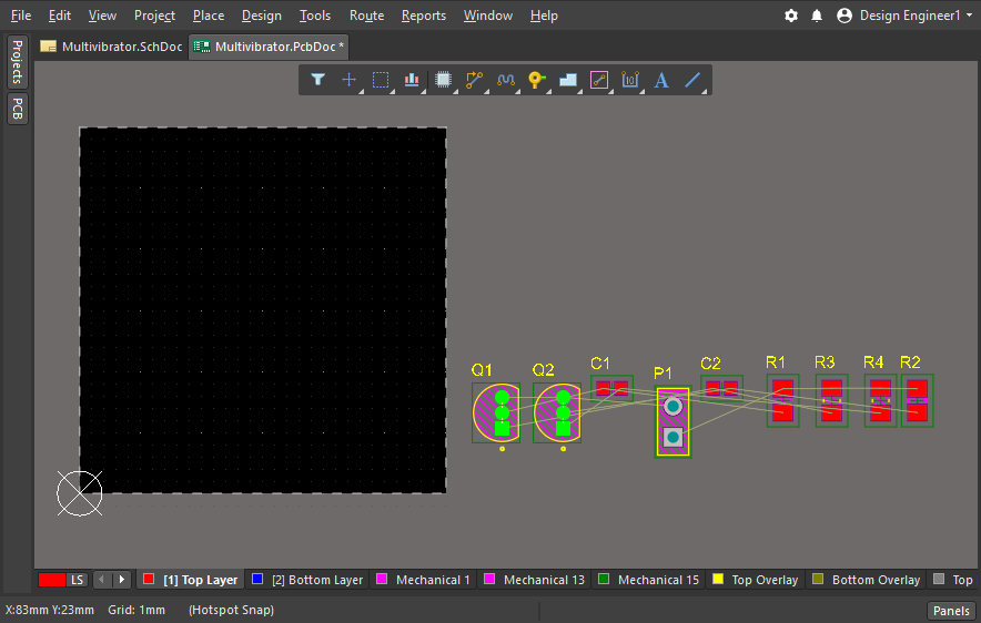
From Idea To Manufacture Driving A Pcb Design Through Altium Designer Altium Designer 18 0 User Manual Documentation

Make Hobbyist Pcbs With Professional Cad Tools By Modifying Quot Design Rules Quot 15 Steps With Pictures Instructables
Spatial resolution of 10 nanometers for precision.
Pcb panel design tool.

Panelize A Round Pcb With Mouse Bites

Pcb Panelizer Gerber Tool Suite This Is Not Rocket Science

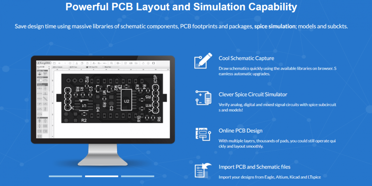
Free Pcb Design Tools Circuitmaker Pcb Design Pcb Design Software Tool Design

How To Do The Pcb Board Array Panelize
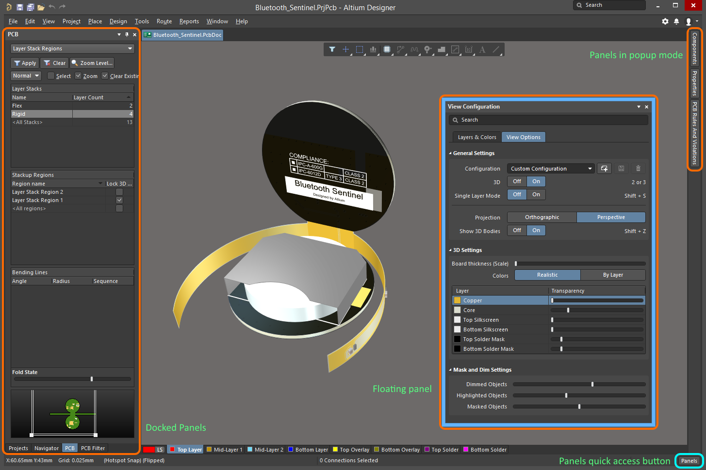
Design Panels Reference Altium Designer 20 2 User Manual Documentation
46 Top Pcb Design Software Tools For Electronics Engineers Pannam
Pads Pcb Design Tutorial Pcbcart

The Best Pcb Antenna Design Software Eases Antenna Implementation

Https Encrypted Tbn0 Gstatic Com Images Q Tbn 3aand9gcqlbnrpll06ikpt07z4vqizei5aqyqhsqf Xa Usqp Cau
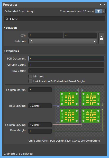
Embedded Board Array Altium Designer 20 2 User Manual Documentation
From Idea To Manufacture Driving A Pcb Design Through Altium Designer Altium Designer 19 0 User Manual Documentation
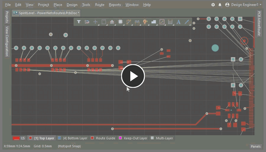
Activeroute Altium Designer 20 2 User Manual Documentation
10 Easy Steps To Design A Circuit Board Altium Designer

10 Free Pcb Design Software Pcb Design Software Pcb Design Software Design
Https Encrypted Tbn0 Gstatic Com Images Q Tbn 3aand9gcsos5hco9ycb2bz Lgbe9mqtfvnxtpz3kqfga Usqp Cau

Forum Easyeda An Easier Electronic Circuit Design Experience Easyeda
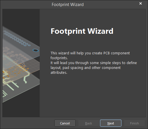
Creating The Pcb Footprint Altium Designer 20 2 User Manual Documentation

How To Make Panelized Pcb In Altium Designer

High Speed Pcb Design Circuit Board Design Pcb Layout Software
Circuit Board Builder Where Is Pcb Inspector In Altium 18
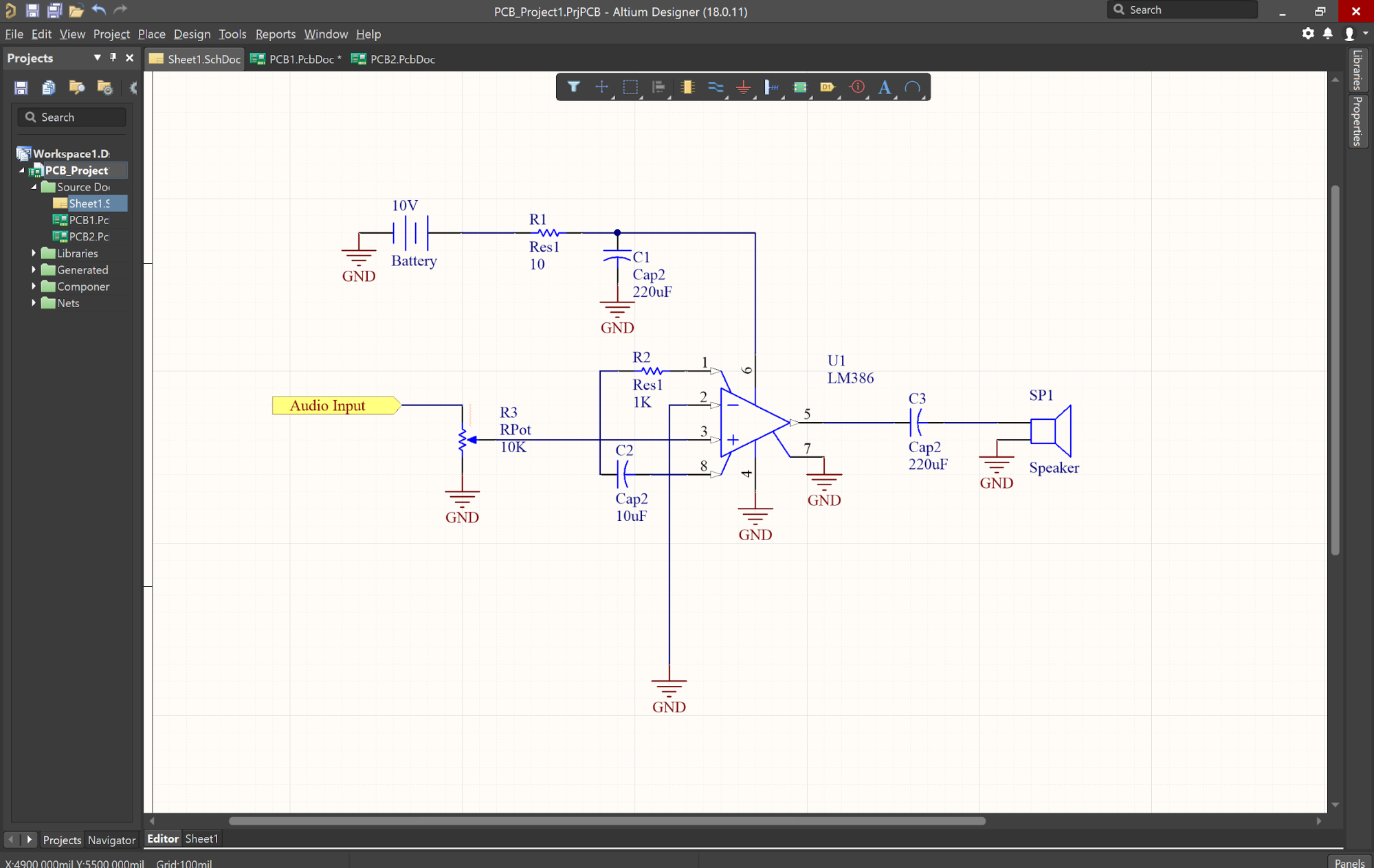
How To Create A Pcb Layout From A Schematic In Altium Designer Pcb Design Blog Altium

How To Export Eagle Pcb To Gerber Files Jlcpcb Help Support
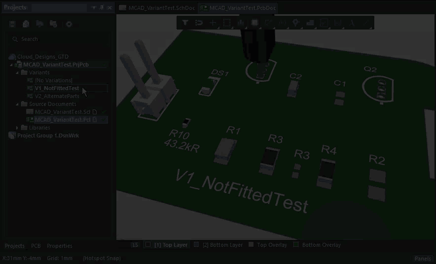
An Introduction To Multi Board Design In Altium Designer Pcb Design Blog Altium Designer
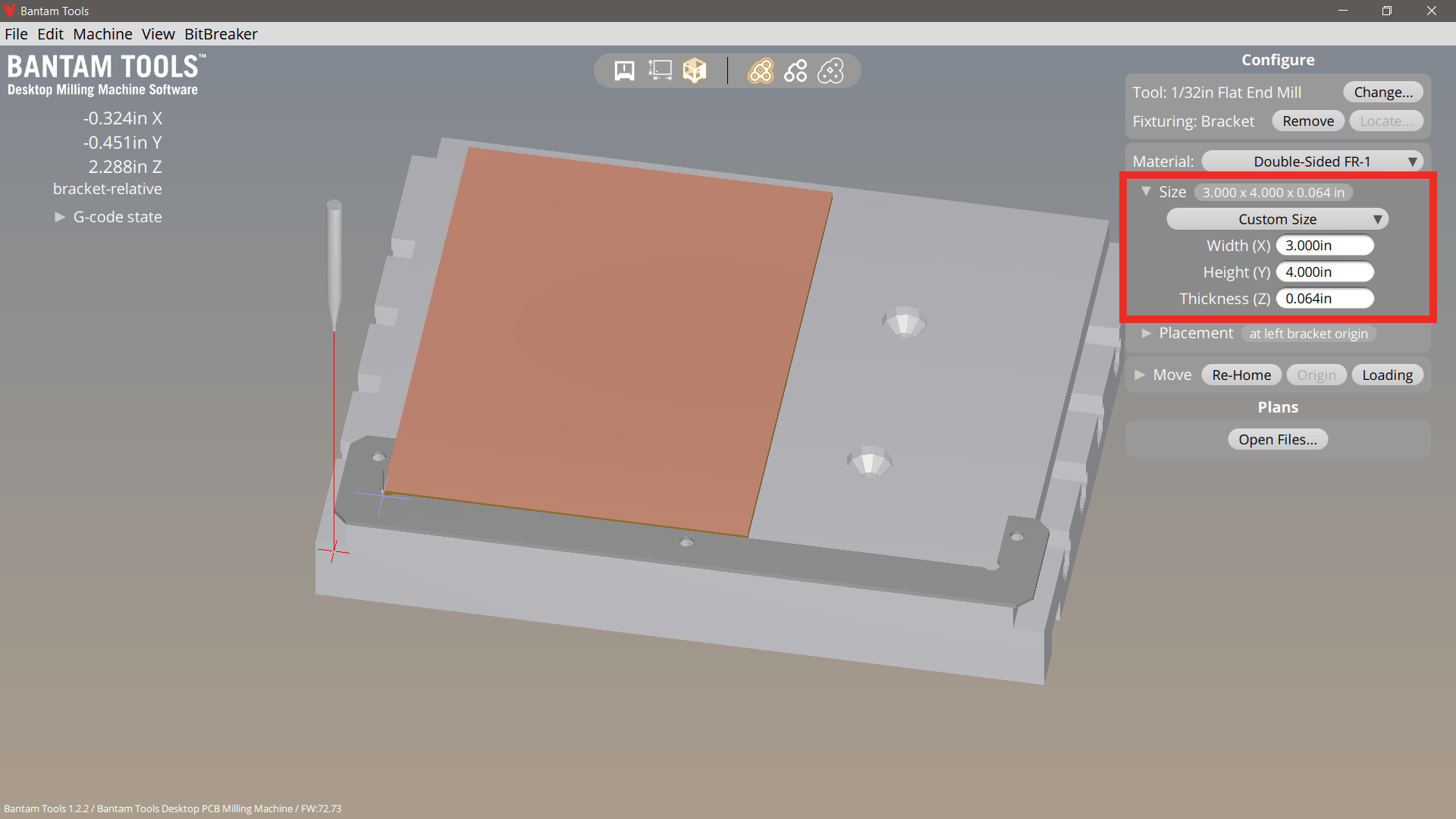
Double Sided Boards Bantam Tools
Source : pinterest.com
